


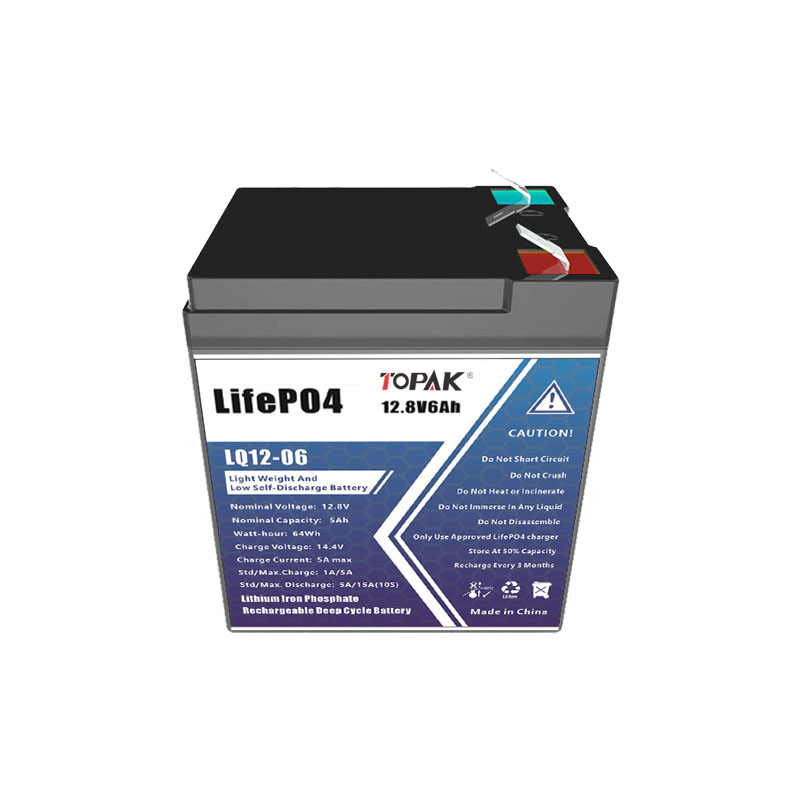
12V 6Ah Lithium ion Battery Lifepo4 Battery
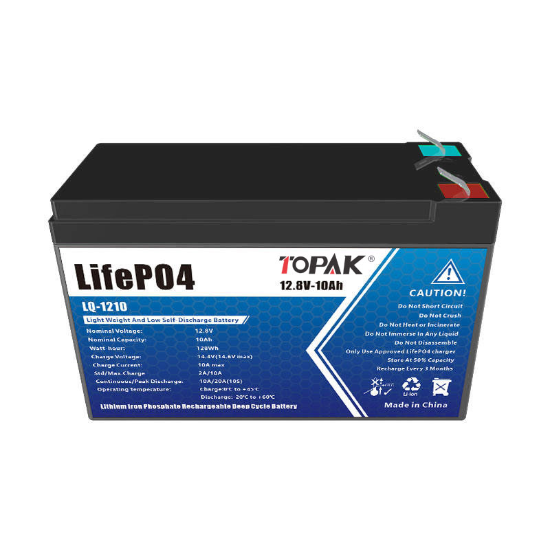
12V 10Ah Lithium ion Battery Lifepo4 Batteries
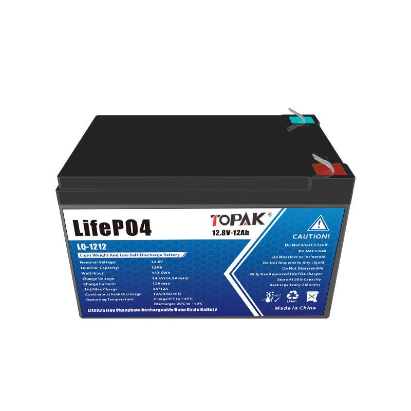
12V 12Ah LiFePO4 Lithium Iron Phosphate Battery
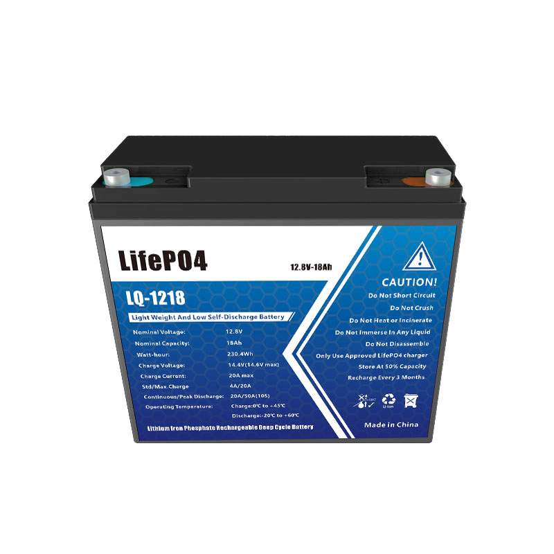
12V 18Ah Lifepo4 Lithium Battery Cell
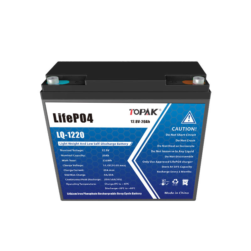
12V 20Ah replacement Lead acid Lithium Battery
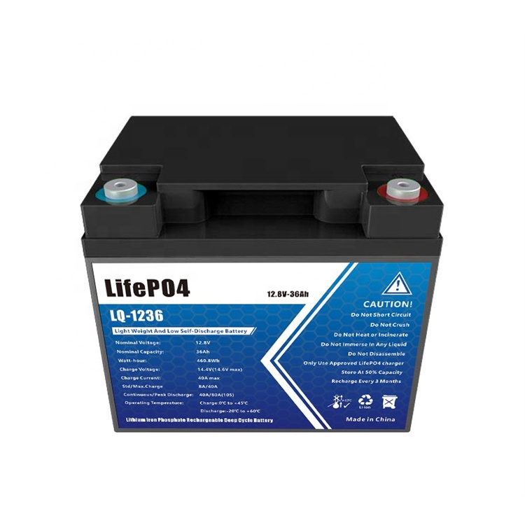
12V 36Ah Lithium Iron Phosphate Battery
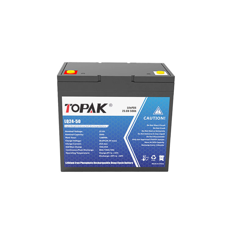
24V 50Ah Lifepo4 Battery Lithium ion Battery
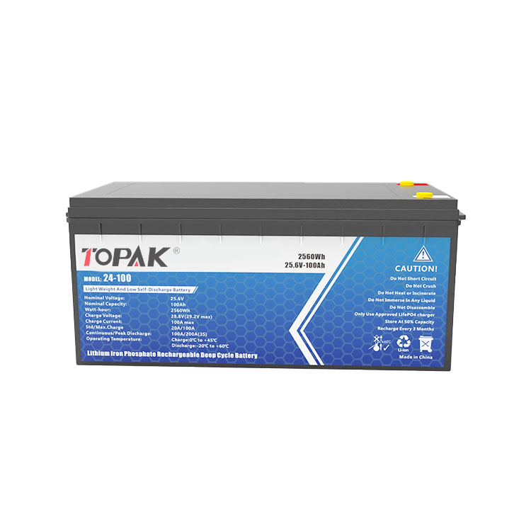
24V 100Ah lifepo4 iron batteries replacement lead acid lithium battery
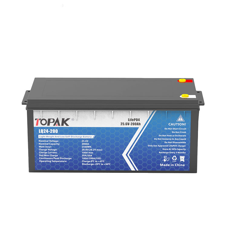
24V 200Ah lifepo4 battery replacement Lead acid Lithium Battery
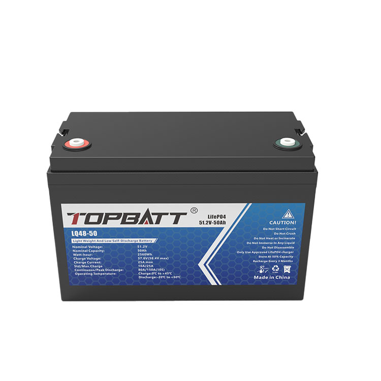
48V 50Ah Lithium Iron Phosphate Battery replacement Lead acid Lithium Battery
48V 100Ah lithium batteries replacement lead acid lithium battery
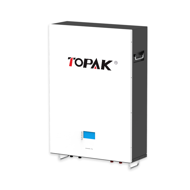
TOPAK 51.2V 300AH Vertical Home Energy Storage Battery
TOPAK 48V 100Ah Home Rack Mounted Energy Storage Batteries
TOPAK 51.2V 100Ah Stackable Battery Shunt able Solar Battery
TOPAK 24V 200Ah Solar Household Wall mounted Battery
48V 1000Ah household Photovoltaic energy storage split type machine
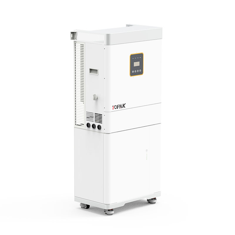
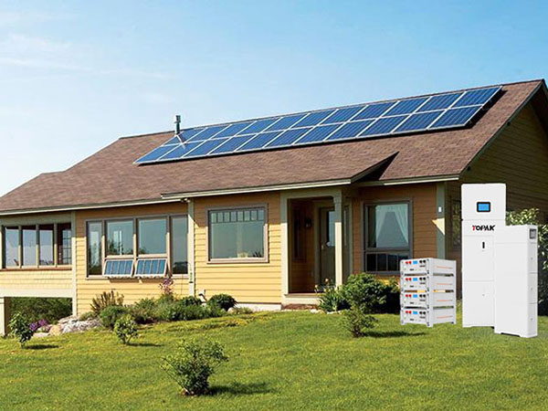
TOPAK 5KWA+5KWh Vertical Home Solar Inverter Energy Storage Integrated Machine Parallelable
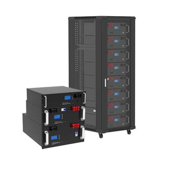
384V 100Ah Backup power supply 38.4kWh UPS Data Center Power System
384V 50Ah Backup power supply 19.2kWh UPS Data Center Power System
192V 100Ah Backup power supply 19.2kWh UPS Data Center Power System
192V 50Ah Backup power supply 9.6kWh UPS Data Center Power System
224V 100Ah UPS Power System 22.4kW LiFePO4 Battery System
TOPAK 224V 30Ah Lithium ion UPS lifepo4 Battery 6.7KW UPS Backup
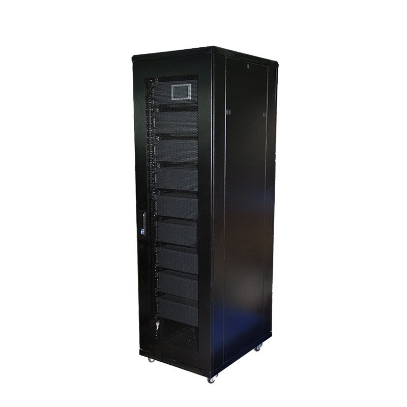
48V 150Ah tower energy stroage battery ofr backup power supply,home/hopital/bank/small business/base station use
48V 100Ah(5U) tower energy stroage battery ofr backup power supply,home/hopital/bank/small business/base station use
Topak tower energy stroage battery for backup power supply,home/hopital/bank/small business/base station use
Topak 48V 100Ah Lithium ion battery BMS Solar Energy Storage System Lifepo4 Battery
48V 200Ah tower energy stroage battery ofr backup power supply,home/hopital/bank/small business/base station use
48V 100Ah(4U) tower energy stroage battery ofr backup power supply,home/hopital/bank/small business/base station use
12V 100Ah Lifepo4 Battery Patent design lithium battery
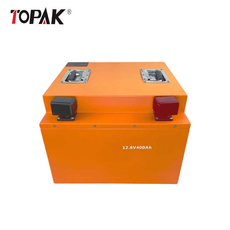
TOPAK RV Lifepo4 Battery 12V 400ah Energy Storage Lithium iron Phosphate RV Battery
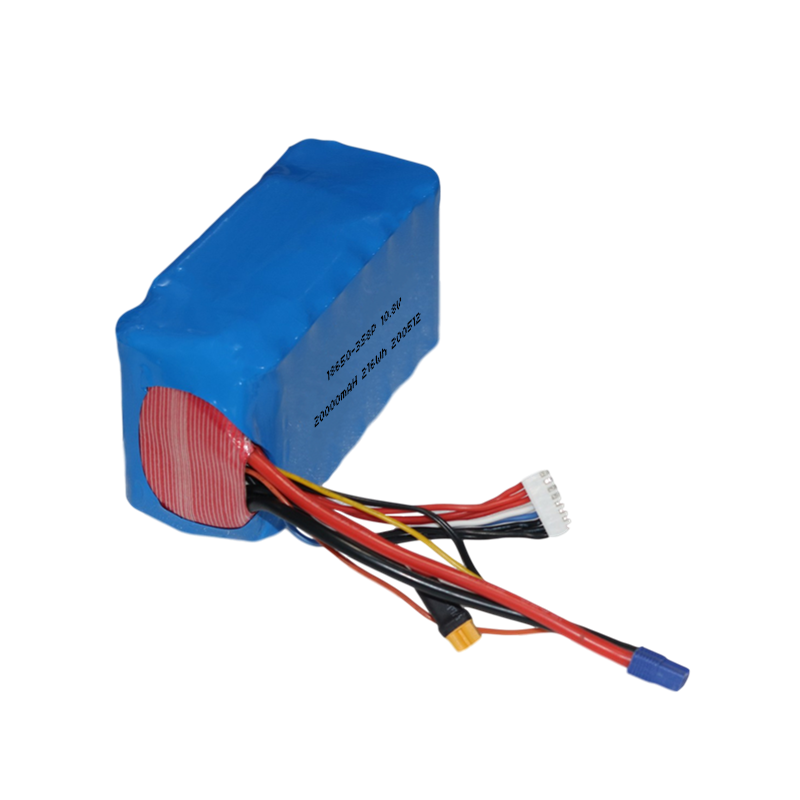
51.2V20AH Lithium battery for electric bicycle battery converter
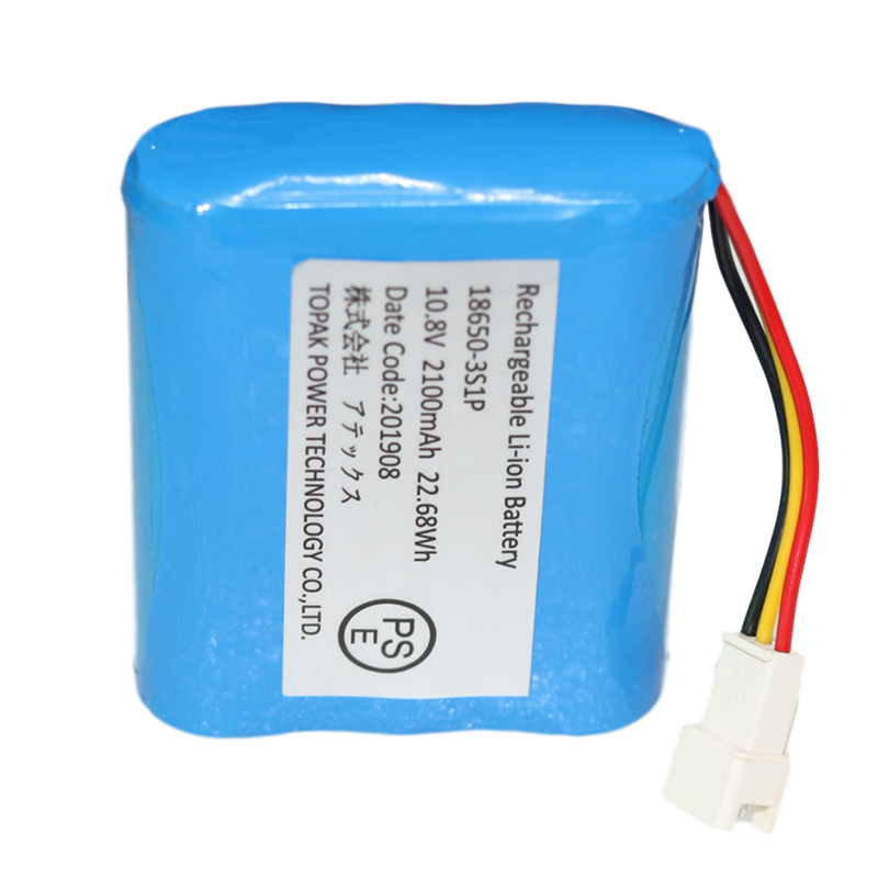
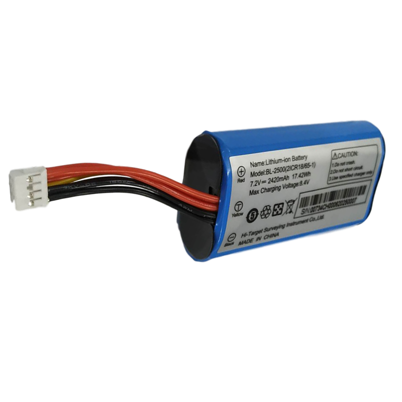
10.8V2.1AH Massager lithium battery
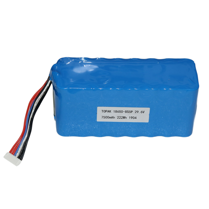
29.6V7.5AH Reserve power supply lithium battery
64V100Ah electric tricycle lithium battery
Writer: TOPAKRelease time: 2020-06-17Page View: 468
One、Background of the case
Surveying and mapping is a long history and very important discipline developed from human production practice, is the basis of national economic development, and is widely used in land, planning, municipalities, construction, geology, geology, highways, railways, oceans, water, military and many other areas. The development of surveying and mapping technology is based on the development of surveying and mapping instruments, especially the modern surveying and mapping technology, which relies on advanced surveying and mapping instruments to a great extent. With the improvement of the economic level and the development of science and technology, China’s electronics industry has been greatly developed, but also to promote the development and application of electronic measuring instruments, electronic measuring instruments occupy an increasingly important position in the electronics industry. A company in June 2019 asked our company to assist in the development of a mapping instrument battery pack, the project is a set of communication, software protection intelligent battery pack; the project has now been delivered in bulk.
Two、Product functions and main features
1. The product has the function of over-charge, over-discharge, over-current, short-circuit, over-temperature and data reading.
2. Charge display
3. SMBus communication interface
4. Adjustable parameter settings
5. Short circuit protection function
6. Integrated IC
7. Low-power, isolated power supply circuit
8. Battery status information reading
Three、Introduction to the overall programme
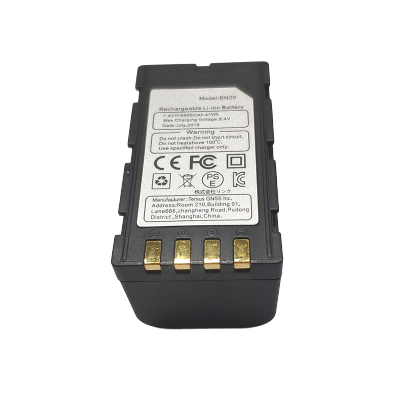
1.Battery parameters: using a brand imported 18650/3200mAh/3.6V battery pack
2.Finished product specifications:18650-2S2P-7.2V-6.4Ah。
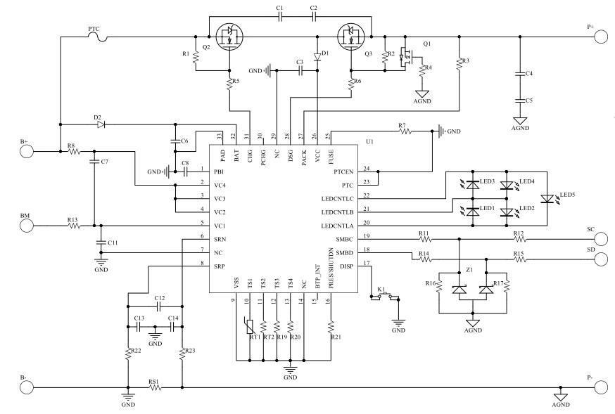
3.Protection board: the parameters and schematic diagram of the smart protection board (SMBus interface communication) are as follows.
4.Assembly process: using 18650-2S2P field structure, reasonable use of space.
Protection parameters:
| No | Item | Condition | Specification |
| 1 | 过充电 Overcharge |
保护电压/Detection voltage | 4.28±0.08V |
| 2 | 保护延迟时间/ Detection delay time | 3.0±0.5S | |
| 3 | 过充恢复 Over charge recovery |
过充恢复电压 Over charge recovery voltage |
4.10±0.1V |
| 4 | 过放电 Over discharge |
保护电压/Detection voltage | 2.75±0.1V |
| 5 | 保护延迟时间/ Detection delay time | 3.0±0.5S | |
| 6 | 充电过流 Over charge current |
充电过流保护电流 Detection Over charge current |
4.0±0.5A |
| 7 | 充电过流保护延时 charge Over current detection delay time |
3.0±1S | |
| 8 | 放电过流 Over discharge current |
放电过流保护电流 Detection Over discharge current |
5.0±0.5A |
| 9 | 放电过流保护延时 Discharge Over current detection delay time |
2.0±1S | |
| 10 | 过放恢复 Over discharge recovery |
过放恢复电压 Over discharge voltage |
3.00±0.1V |
| 11 | 短路保护 | 恢复条件/Release Conditions | 断开负载/充电激活Disconnect load/charge activation |
| 12 | 充电温度保护 Overtemperature in Charge Protection |
充电高温保护 Overtemperature |
65±2℃ ,delay 3S |
| 解除温度 Overtemperature release |
45℃±5℃,delay 3S | ||
| 充电低温保护 Undertemperature |
-5±2℃,delay 5S | ||
| 解除温度 Overtemperature release |
0±5℃,delay 5S | ||
| 13 | 放电温度保护 Overtemperature in Discharge Protection |
放电高温保护 Overtemperature |
65±3℃ ,delay 3S |
| 解除温度 Overtemperature release |
55℃±5℃,delay5S | ||
| 放电低温保护 Undertemperature |
-40±5℃,delay 5S | ||
| 解除温度 Overtemperature release |
-35±5℃,delay 5S | ||
| 14 | 建议工作条件 Suggest working conditions |
建议工作温度/suggest working temperature | -20℃~+60℃ |
| 15 | 内阻/IR resistance | PCM内阻/ IR of PCM | ≤50.00 mΩ |
Schematic:
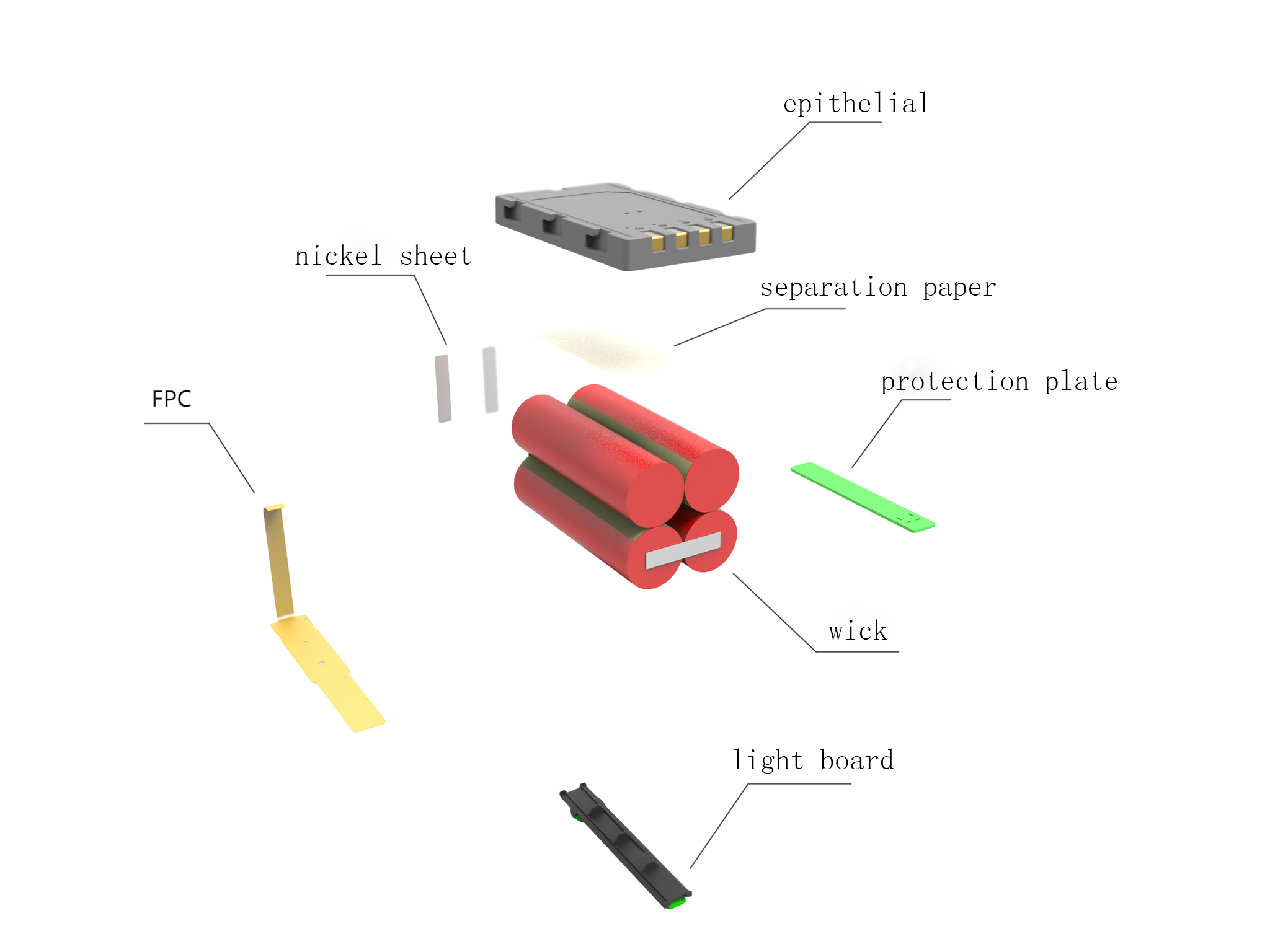
Four、Product’s BOM
| NO | Item | Criteria |
| 1 | Semi-manufactured cell | 18650 3200mAh |
| 2 | PCM | TOPAK-929/C1340/BQ40Z50R1/ 2 strings / with LED indication / FPC |
| 3 | Shell-1 | L*W*H=70*40*34MM,epithelial |
| 4 | Shell-2 | L*W*H=70*40*7.8MM,sump |
| 5 | Key | Φ*H=9*1.4MM,Round/Keypad |
| 6 | Key pads | Φ*H=12*1.5MM,C1340/Round/Key Pad |
| 7 | support | L*W*H=66.5*10.6*6.3mm,C1340,Long stand/black |
| 8 | Label | T*W*L=0.1*29.7*47.6mm/Silver/PC surface lamination, matte finish |
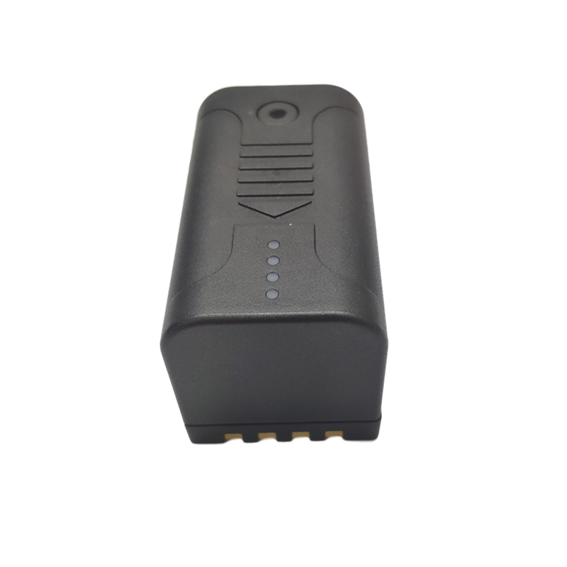
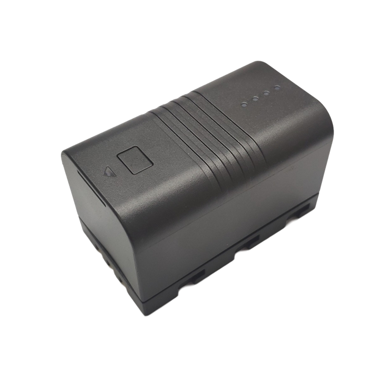
Five、Product size and effect display diagram
bomb map
Pictures of the finished product
ShenZhen Topak New Energy Technology CO.LTD.
+86 13688963831
B2B@topakpower.com
Address: 26 Yingfeng 1st Road, Dalang Town, Dongguan City, Guangdong Province (Tuopai Industrial Park)


Copyright © 2019 Shenzhen topak new energy technology CO.LTD. 粤ICP备20054061号